
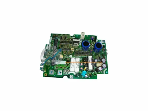
FUJI
FUJI G11-PPCB-4-1.5 SA528530-06 Replacement for FRENIC G11
G11-PPCB-4-1.5 SA528530-06FUJI G11-PPCB-4-1.5 SA528530-06 replacement power PCB for FRENIC G11 drives. Compatible upgrade, 12-month warranty, fast shipping. SKU: SA528530-06.
Request availability, condition, lead time and export shipping details for SA531121-02 E11-C4PCB.
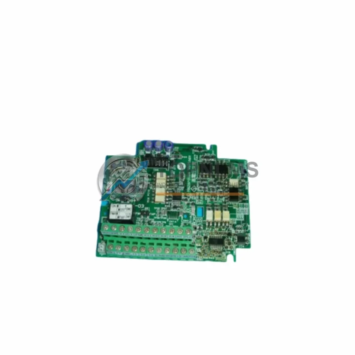
Send this exact part number, quantity and destination country. TOPNLMS will confirm availability, condition and export lead time before quotation.
When your FUJI FRENIC series inverter drive board fails or reaches end-of-life, unplanned downtime can cascade across your entire production line. The SA531121-02 E11-C4PCB is the OEM drive control PCB used across multiple FRENIC inverter platforms, and sourcing a verified replacement quickly is critical for facilities running continuous or semi-continuous processes. TOPNLMS maintains ready stock of the SA531121-02 E11-C4PCB, fully tested and shipped with a 12-month warranty, to support your retrofit, emergency replacement, or planned upgrade program.
This drive board is engineered for direct installation into FRENIC-series inverter chassis without modification to the existing wiring harness, terminal block layout, or control cabinet footprint. Whether you are replacing a failed unit in a FRENIC-Multi, FRENIC-Eco, or FRENIC-Mini platform, the SA531121-02 E11-C4PCB maintains full compatibility with the original gate drive signals, feedback circuits, and protection logic already present in your inverter assembly.
| Parameter | Legacy / Outgoing Board | SA531121-02 E11-C4PCB (Replacement) |
|---|---|---|
| Part Number | Earlier FRENIC drive PCB revisions | SA531121-02 E11-C4PCB |
| Compatible Platform | FRENIC-Multi, FRENIC-Eco, FRENIC-Mini | FRENIC-Multi, FRENIC-Eco, FRENIC-Mini |
| Mounting Interface | OEM PCB standoff pattern | Identical OEM standoff pattern — no drilling required |
| Connector / Terminal | Original FUJI ribbon and JST connectors | Fully compatible — plug-and-play replacement |
| Gate Drive Signal | IGBT gate drive, OEM spec | Matched gate drive timing and voltage levels |
| Communication Protocol | Internal inverter bus (RS-485 / proprietary) | Compatible with existing inverter control bus |
| Protection Functions | OC, OV, UV, OH, GF | Full protection parity: OC, OV, UV, OH, GF |
| Power Supply Requirement | Internal SMPS from inverter chassis | Powered by existing chassis SMPS — no external supply needed |
| Installation Space | Standard FRENIC inverter bay | Same form factor — no cabinet modification required |
| Replacement Recommendation | Discontinue legacy revision | Direct drop-in replacement recommended |
| Warranty | — | 12-Month Warranty from TOPNLMS |
A successful FRENIC inverter drive board replacement rarely involves a single component in isolation. In practice, field engineers replacing the SA531121-02 E11-C4PCB often find it necessary to inspect or simultaneously replace adjacent components to ensure the repaired inverter returns to full specification. The IGBT power module stack — typically a FUJI 2MBI or 6MBI series module — should be tested for gate-emitter leakage before reinstalling the new drive board, since a degraded IGBT module is frequently the root cause of drive PCB failure. Similarly, the DC bus capacitor bank within the inverter chassis should be checked for capacitance and ESR drift, as aged capacitors can stress the new board’s protection circuits immediately after commissioning.
For facilities running multiple FRENIC inverters on the same production line, it is common practice to maintain a small buffer stock of the FRENIC control terminal board (option card interface PCB) alongside the drive board, since both boards share the same internal bus and a fault on one can induce transient stress on the other. If your inverter is equipped with a FUJI OPC-G1-RJ option card for PROFIBUS or DeviceNet communication, verify that the option card firmware revision is compatible with the replacement drive board before powering up — mismatched firmware revisions between the option card and the main drive PCB have been known to cause initialization faults on FRENIC platforms.
Control cabinet wiring should also be reviewed during the replacement process. The FUJI TP-G1 remote keypad cable and the keypad itself are often overlooked during drive board swaps, but a damaged keypad cable can introduce noise on the control signal lines and trigger nuisance trips on the newly installed board. If your system uses a FUJI FRENIC parameter loader or PC tool for parameter backup and restore, ensure that all inverter parameters are backed up before removing the failed board, as some FRENIC models store a subset of parameters in the drive PCB’s onboard EEPROM rather than in the control board.
For sites migrating from older FRENIC-G11 or FRENIC-P11 platforms to current FRENIC-Multi or FRENIC-Ace architecture, the SA531121-02 E11-C4PCB replacement project is often the trigger for a broader system review. In these migration scenarios, engineers typically also evaluate the FUJI FRENIC-Ace FRN series main control board, the associated keypad display unit, and the braking resistor unit to confirm that the upgraded inverter assembly meets the new system’s dynamic braking requirements. If the application involves a multi-drive system with a common DC bus, the bus bar connections and the shared DC reactor should be inspected at the same time to prevent nuisance overcurrent trips after the drive board is replaced.
Q: Do I need to re-wire the control terminals after replacing the SA531121-02 E11-C4PCB?
A: No. The SA531121-02 E11-C4PCB is a direct drop-in replacement for the original FUJI FRENIC drive board. All existing control wiring, terminal block assignments, and shielding arrangements remain unchanged. Simply disconnect the original board’s ribbon cables and JST connectors, remove the board from its standoffs, seat the replacement board, and reconnect all cables in the original configuration.
Q: Will my existing inverter parameters be retained after the board swap?
A: Parameters stored in the FRENIC control board’s EEPROM are typically retained on the control board, not the drive board. However, TOPNLMS strongly recommends performing a full parameter backup using the FUJI FRENIC Loader software or the TP-G1 keypad before beginning any board replacement, as a precautionary measure against unexpected parameter loss during power cycling.
Q: Is the SA531121-02 E11-C4PCB compatible with RS-485 Modbus RTU communication?
A: Yes. The FRENIC series inverter’s RS-485 Modbus RTU communication function is managed by the control board and option card, not the drive board. Replacing the SA531121-02 E11-C4PCB does not affect the inverter’s communication configuration, register mapping, or baud rate settings. Your existing SCADA or PLC communication setup will continue to operate without modification.
Q: What is the physical installation procedure for the replacement board?
A: Power down the inverter and wait a minimum of 10 minutes for the DC bus capacitors to discharge to a safe voltage (below 30 VDC, verified with a multimeter). Remove the inverter front cover and locate the drive board. Photograph the cable routing before disconnection. Remove all ribbon cables and JST connectors from the original board. Unscrew the four PCB standoff screws, remove the original board, and seat the SA531121-02 E11-C4PCB replacement. Reconnect all cables in the original routing, replace the front cover, and perform a no-load test run before reconnecting the motor load.
Q: Can this board be used in a FRENIC inverter that drives a high-inertia load such as a centrifuge or large fan?
A: Yes. The SA531121-02 E11-C4PCB supports the full range of FRENIC inverter protection and control functions, including extended deceleration time settings and dynamic braking control signals. For high-inertia applications, verify that the braking resistor unit and braking transistor are in good condition before commissioning the replacement board, as these components are subject to additional thermal stress in high-inertia deceleration cycles.
Q: What if my inverter chassis has a different revision of the drive board installed?
A: Minor PCB revision differences within the FRENIC drive board family are common across production batches. The SA531121-02 E11-C4PCB is the current production revision and is backward compatible with earlier FRENIC chassis revisions. If you are uncertain about compatibility for a specific chassis serial number range, contact TOPNLMS with your inverter nameplate data and we will confirm compatibility before shipment.
Every SA531121-02 E11-C4PCB shipped by TOPNLMS is covered by a 12-month warranty from the date of delivery. Prior to shipment, each board undergoes a multi-point outgoing inspection that includes visual inspection for component damage, solder joint integrity check, connector seating verification, and a functional power-on test where applicable. Boards that do not pass inspection are quarantined and not shipped.
In the event of a warranty claim, TOPNLMS provides a replacement unit or full refund, depending on the customer’s preference and stock availability. Warranty claims are processed within 3 business days of receiving the returned unit. Return shipping for confirmed warranty defects is covered by TOPNLMS for orders shipped within mainland China; international warranty return logistics are handled on a case-by-case basis with the customer’s freight forwarder.
For urgent replacement scenarios where production downtime cannot be tolerated, TOPNLMS offers advance replacement shipment for qualified accounts — a replacement board is shipped before the defective unit is returned, subject to a refundable deposit. This service is available for customers with established purchase history or upon receipt of a purchase order for the replacement unit.
Stock availability is updated in real time. Orders placed before 16:00 CST on business days are processed for same-day dispatch. International orders are shipped via DHL Express, FedEx International Priority, or SF International, with tracking provided at the time of dispatch. Estimated transit times are 3–7 business days to most destinations in Southeast Asia, Europe, and the Americas.
For procurement inquiries, bulk pricing, or technical pre-sales support, contact the TOPNLMS team directly:
📧 [email protected] | 📞 +86 18359293191
FUJI G11-PPCB-4-1.5 SA528530-06 replacement power PCB for FRENIC G11 drives. Compatible upgrade, 12-month warranty, fast shipping. SKU: SA528530-06.
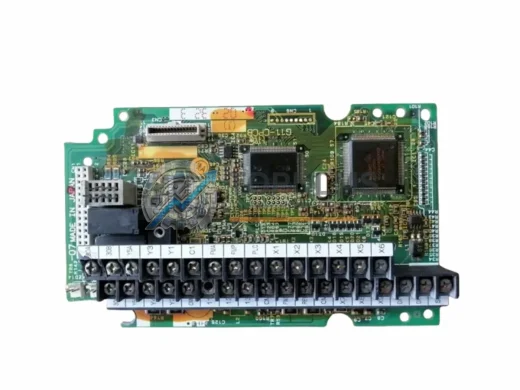
Original FUJI G11-CPCB SA529591-08 control CPU board for Frenic G11 VFD series. Direct replacement, 12-month warranty, tested before shipment. Industrial stock available.
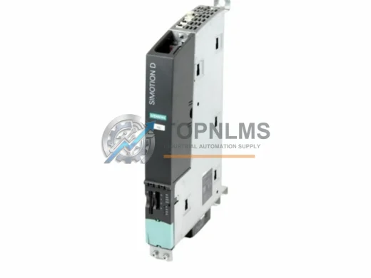
Siemens 6AU1425-0AA00-0AA0 SINAMICS S120 D425 ruggedized drive control unit. In stock, tested, 12-month warranty. Fast global shipping from TOPNLMS.
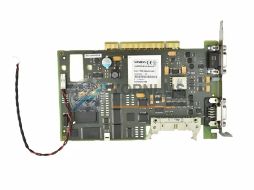
Siemens 6AU1390-0AA00-0AA1 A5E00442198 SIMODRIVE servo control module replacement. Drop-in upgrade, wiring-compatible, 12-month warranty. Ships from stock.
Click Quote This Model and the Part Number field will auto-fill with SA531121-02 E11-C4PCB.